One of the entries in NASA/JPL's otherwise-excellent Deep Space Network FAQ is, "I am an Amateur Radio operator. Can I listen to the data coming from (interplanetary) spacecraft?"
The answer, according to the FAQ, is "Unfortunately, no." But a growing community of Amateur Radio hobbyists has taken exception to NASA's pessimistic attitude. As of this writing (November 2007), X-band signals from probes including Venus Express and the Mars Reconnaissance Orbiter are being received by amateurs using relatively-modest antennas. Reception of the Cassini probe at Saturn has been reported via a 165-cm dish. These efforts have culminated in successful Amateur reception of no less a DX target than Voyager 1, the most distant object ever built by mankind.
While the March 2006 QSO with Voyager took place on a borrowed 20-meter dish at Bochum Observatory, the feat was soon duplicated by Luis Cupido, CT1DMK using his own 5.6-meter dish. As Luis's page shows, signals from essentially all of the major deep space missions are accessible to the serious microwave enthusiast.
A recent discussion on the WA1MBA microwave list raised the topic of local-oscillator performance requirements for amateur DSN work. Excellent close-in phase noise and residual FM are important here due to the narrow signal bandwidths in use. Traditionally, commercial microwave "brick" sources have provided LO signals for most Amateur DSN actiivty. These components are far too expensive for most hobbyists to purchase new, so the surplus/eBay marketplace is usually the first (and last) resort.
This project grew out of a belief that inexpensive, off-the-shelf PLL chips were also up to the task of generating DSN-grade LO signals. Beyond the obvious educational value, our ability to design and construct economical microwave synthesizers for arbitrary output frequencies gives the ham community something else in common with NASA: we're no longer at the mercy of the surplus market!
Download: All project files created with CadSoft EAGLE 4.16r2
Download: Four-layer Gerber and drill files only, suitable for submission to BatchPCB.com
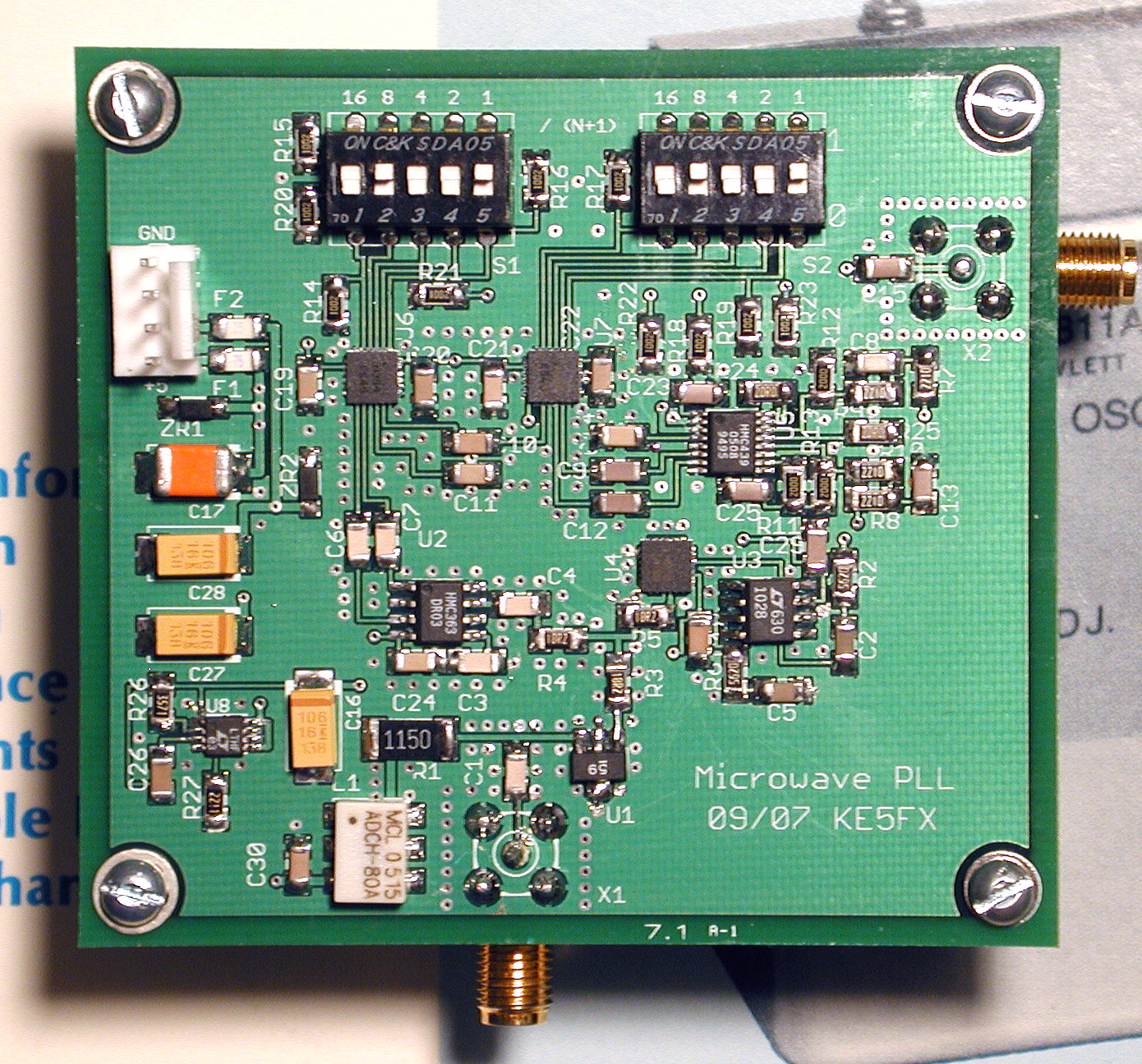
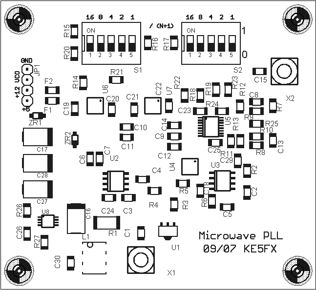
Project components
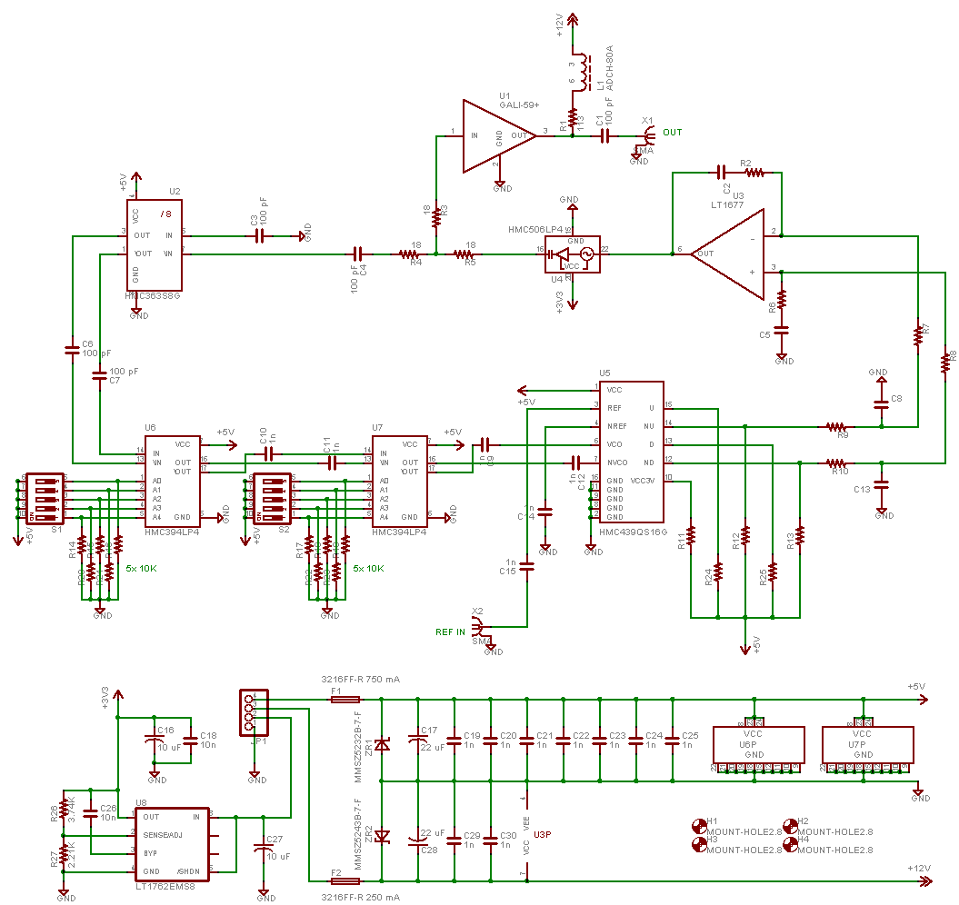 The synthesizer described here is a basic single-loop PLL constructed with chips from the Hittite Microwave
product line, notably the HMC439 phase-frequency detector
and HMC506 VCO. The HMC506 tunes from 7.8 to 8.7 GHz, but any of several microwave VCOs in the same
package style can be used, subject to the HMC363 prescaler's 12 GHz input frequency specification.
The VCO has its own supply regulator on the board, a low-noise LT1762.
The synthesizer described here is a basic single-loop PLL constructed with chips from the Hittite Microwave
product line, notably the HMC439 phase-frequency detector
and HMC506 VCO. The HMC506 tunes from 7.8 to 8.7 GHz, but any of several microwave VCOs in the same
package style can be used, subject to the HMC363 prescaler's 12 GHz input frequency specification.
The VCO has its own supply regulator on the board, a low-noise LT1762.
The HMC363, with its fixed division modulus of 8, drives a pair of 2.2-GHz HMC394 counters that are programmed with 5-bit DIP switches. This means the loop can support any division ratio that results in an output frequency within the VCO's tuning range, as long as the ratio can be written as the product of the prescaler factor (8) and two independent 5-bit terms (actually 2 to 32, since division ratios of 1 are not supported).
In practice, the DIP switches are programmed with the counter's division factor minus one; for instance, N=80 (8*10) would be achieved by programming the DIP switches for 5-1 and 2-1, or 4 and 1. N=800 could be programmed in several ways, the most obvious being 8*10*10 with both DIP switches set to 9.
The unlabelled resistors and capacitors on the schematic are loop filter components whose values depend on the PLL's desired output frequency and division factor. The PLL Calculator on the Hittite home page is easy to use and doesn't require any further explanation here, except to point out that the HMC506 is a relatively-noisy VCO, owing to its high tuning sensitivity. It benefits from the use of a wide loop bandwidth, on the order of 80-200 kHz.
Theoretical noise characteristics
The HMC439 accepts an input reference at frequencies ranging from 10 MHz to 1300 MHz, much wider than competing CMOS PLLs from companies such as Analog Devices and National Semiconductor. On paper, these manufacturers' CMOS PLL products offer numerous advantages over competing Hittite GaAs HBT products, including much-lower power consumption, many more features including integrated counters and programming logic, and lower cost. However, the Hittite parts are "quieter" at the high comparison frequencies I wanted to work with in this case.
An example is helpful. With a division ratio (N) of 80, which would be used to synthesize an 8000 MHz output signal based on a 100-MHz comparison frequency, the theoretical phase-noise floor of a loop constructed with Analog Devices' ADF4108 is -219 dBc/Hz + 20*log(80) + 10*log(100000000) dBc/Hz, or -101 dBc/Hz. The same loop constructed with the HMC439 phase-frequency detector and various counters from the same product line would be capable of performance in the -114 dBc/Hz neighborhood, based on the graph on page 2 of the data sheet which appears to have the 10*log(Fcomp) term "baked in."
Either of these figures would be more than adequate for our purpose -- the 8-GHz band isn't exactly crowded. The Analog Devices parts would have served well, but I had another purpose in undertaking this project: to find out if I could successfully install the Hittite chip-scale packages at home without investing in a professional reflow oven. The future of the hobby may well hang on this question, because more and more interesting ICs are being produced only in leadless chip-scale packages these days. How are you supposed to solder a connection at 40 or more pins per inch that you not only can't reach, but you can't even see?
Assembly
The soldering technique I chose was definitely a low-tech one. A tube of Kester Sn63/Pb37 solder paste from Digi-Key and a dental pick allowed me to spread a thin layer of solder over the rows of pads where the Hittite chips would be installed. I placed the chips on the pads with tweezers, centering them as best I could... then blasted the board with a 1500-watt heat gun, held a few inches beneath it.
The solder melted and flowed away from the gaps between the pads in about 20-30 seconds. I continued to apply heat for another five seconds or so, tapping gently on the board to encourage the parts to center themselves via surface tension, then withdrew the heat gun. Only one visible solder bridge resulted from this process; it was easily removed with solder wick and a sharp iron tip pressed up against the edge of the affected IC. But how many more solder bridges had formed beneath the ICs?
Thanks to my dentist's contribution of some time with his CCD X-ray imager, I was able to see that while many of the pads had a small amount of excess solder on them, no obvious trouble spots existed between the pads. A low-current continuity test with a DMM also failed to turn up any additional bridges... and the board worked the first time.
I'm reasonably happy with this process, even though it wasn't a good feeling to see my new PCB smoking before I'd even applied power to it. While it's unlikely that this crude procedure conforms to any manufacturer's idea of a proper reflow profile, the heat gun-and-solder paste technique appears to be a reasonably quick, simple, and inexpensive way to solder chip-scale packages at home. But I won't call it "reliable" until I've done quite a few more boards. And I want my own X-ray machine now, dammit!
Output power and flatness
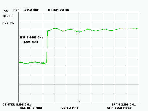 At left is a graph of the board's output power versus frequency, taken by applying a 1-11 volt ramp to the VCO's
tuning line. Observed flatness was very good, but the power output level wasn't what I was hoping for.
Mixers generally need
+7 to +10 dBm at their LO ports, but the synthesizer is only generating about -2 dBm at 8 GHz. That means that an external
amplifier stage will be needed in a receiving system that uses this board. What went wrong?
At left is a graph of the board's output power versus frequency, taken by applying a 1-11 volt ramp to the VCO's
tuning line. Observed flatness was very good, but the power output level wasn't what I was hoping for.
Mixers generally need
+7 to +10 dBm at their LO ports, but the synthesizer is only generating about -2 dBm at 8 GHz. That means that an external
amplifier stage will be needed in a receiving system that uses this board. What went wrong?
The HMC506 VCO itself is rated for +14 dBm output, and the Mini-Circuits GALI-59+ MMIC at the output should have provided enough gain at 8 GHz to make up for the resistive splitter between the VCO, prescaler, and MMIC input. It's true that FR-4 PCB material is somewhat lossy at 8 GHz, but only on the order of 1 dB/inch (Bogatin, Signal Integrity Simplified, 2004, p. 380).
Discussion on the WA1MBA list leads me to suspect inadequate clearance between the 8-mil-wide traces and the surrounding top-layer ground plane. I believe that a combination of this factor and additional loss in the Y-network is responsible for most of the power deficit. Standard 1206 resistors aren't well-characterized for use at 8 GHz, and neither is the GALI-59+ for that matter.
My next version of the PC board will open up much more clearance to the microstrip traces, and
I'll also switch to the new HMC311 amplifier.
The HMC311 and GALI-59+ have similar gain specs at 8 GHz (approximately 11 dB), but the HMC311 is capable of at least +8 dBm output
at that frequency while the GALI-59+ is probably compressing at 3-4 dBm, judging by its S21 graph.
Broadband spectral purity
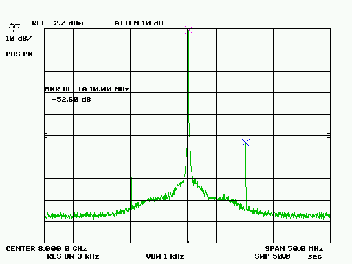 Overall spectral purity in this plot -- taken with the loop configured for a 10 MHz reference -- is excellent, although
the reference spurs were somewhat higher than I'd expected. This is not a problem in the board's intended application, since there
are few other signals in the microwave bands to cause spurious responses.
Overall spectral purity in this plot -- taken with the loop configured for a 10 MHz reference -- is excellent, although
the reference spurs were somewhat higher than I'd expected. This is not a problem in the board's intended application, since there
are few other signals in the microwave bands to cause spurious responses.
With the loop configured for a 100 MHz reference, no spurs (reference or otherwise) were observed.
Phase noise
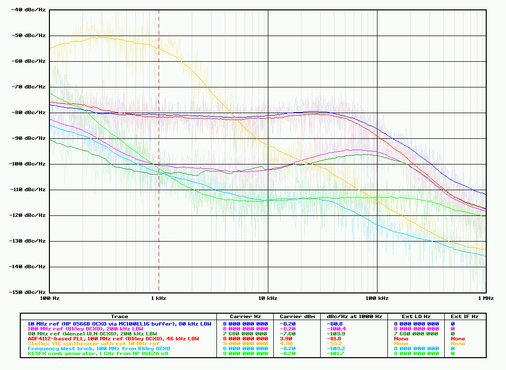
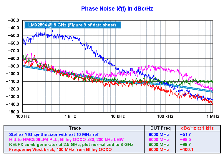
Observed noise performance is quite good. Viewed above are some plots taken with an HP 11729C/8662A/8566B phase-noise measurement
system running PN.EXE from the KE5FX GPIB Toolkit.
The blue and red traces show that with a reference frequency of 10 MHz, performance of the Hittite-based synthesizer is similar to that of an HMC506-based synthesizer constructed with an Analog Devices ADF4112 PLL chip (Fcomp=2.0 MHz, design frequency=2.0 GHz, external prescaler=4x; ADISimPLL file downloadable here). These traces are also close to the noise level predicted by the Hittite PLL Calculator simulation.
About the only reason to use the Hittite PLL and counter chips with a 10-MHz reference would be for an application where no microcontroller or PC was available to program the Analog Devices part. Otherwise, the CMOS parts are, again, much better from the standpoints of power consumption and programming versatility.
The green and purple traces were taken with the DIP switches configured to multiply 80 MHz by 96 (7.68 GHz) and 100 MHz by 80 (8.0 GHz), respectively. These higher reference frequencies give the Hittite parts a chance to show what they're made of.
7.68 GHz is technically out of the HMC506 VCO's specified range, but it is interesting to test the PLL at this frequency because it allows the use of an 80-MHz ultra-low-noise Wenzel OCXO as a reference. The Wenzel OCXO is quieter than the Bliley BECO OCXO I normally use as a 100-MHz reference source.
At 7.68 GHz, the Hittite PLL's close-in phase noise is approximately -91 dBc/Hz at 100 Hz from the carrier. This is within one dB of the figure obtained by adding 20*log(96) (40 dB) to the -132 dBc/Hz specification for the Wenzel OCXO at 100 Hz. A similar result is obtained by adding 20*log(768) (58 dB) to the 100-Hz specification (-150 dBc/Hz) of the 10-MHz HP 10811A in the phase-noise test set. At offsets beyond a few hundred Hz, of course, the PLL's noise floor is no longer dominated by its reference.
Executive summary: at offsets close to the carrier, the phase noise of this PLL is good enough to take advantage of some the best crystal oscillators available. Beyond 1 kHz, other sources such as an 8-GHz Frequency West brick (blue) and comb generator (bright green) are quieter.
Broadband noise performance is not as impressive, compared to either the Stellex YIG synthesizer (yellow) or Frequency West brick traces. This result is not surprising given the specifications of the HMC506 VCO. Analog Devices obtained similar broadband performance with the HMC506 in their ADF4108 data sheet (figure 7). Better filtering at the LT1762 output could help here, because these results are 10-15 dB worse than the HMC506 VCO's specification at 100 kHz.
Another likely candidate for addition to the circuit is a final RC pole between the opamp and the VCO tuning line. Slight noise peaking at offsets near 10 MHz was noted with the
100-MHz loop design; it was cleared up with a 470-ohm series resistor. With its sensitivity of 160 MHz/volt at 8 GHz, the HMC506 VCO needs
the cleanest tuning signal it can get.
Additional notes and correspondence
November 5, 2007 You can order boards to reproduce this project from BatchPCB by submitting
the zipfile at the top of the page to them. (I will not be selling boards or parts personally, or maintaining a BOM.) Each board is about US $90.00 in quantities of one, with typical
delivery time around 4 weeks. The current PCB works well, but keep in mind that I will probably revise it within a few months to address issues noted above.
A parts-placement diagram can be found here.
Current consumption is about 600 mA at +5V, 65 mA at +12V, and 100 mA on the VCO supply pin (which should be connected to +5 to +8 VDC; more than that will cause the LT1762 to run hot.) The +5V supply is relatively-critical; it needs to be between +4.9 and +5.1V. The 750 mA fuse drops about 0.2-0.3V, which makes a 4.9V supply marginal for operating the Hittite parts. Above +5.1V, the HMC394 counters run somewhat hotter than I prefer. It's likely that additional solder on their ground tabs, and possibly another via or two to the ground plane, would help.
The Hittite parts require fast edges at their inputs, including the reference input of the HMC439 phase-frequency detector. This means that more drive power is required from 10 MHz reference sources than from 100 MHz sources. The board needs at least +9 dBm for reliable operation with a 10 MHz reference, while 0 dBm should be sufficient at 100 MHz.
It's a good idea to run the power-supply leads through a ferrite and possibly add a few
extra bypass capacitors at the Molex connector on the PC board, as well as where the supply leads enter the board's enclosure if one is used.
The board is fairly sensitive to EMI on the power-supply lines.
December 15, 2011: In the four years since this page was originally written, a lot of good, cheap options for reflow soldering at home have emerged. For a few hundred dollars you can buy a proper hot-air soldering tool and
(even more important) a preheater. In combination, these tools allow you to approximate industry-standard reflow temperatures and timing profiles,
avoiding the unnerving smoking-PCB phenomenon.
I currently use an Aoyue 2738int hot-air repair station for SMT assembly and rework, along with an Aoyue 853A quartz preheater... but there are numerous other options, depending on when you go shopping and how much you're looking to spend. Some excellent tutorials can be found on YouTube and sites such as SparkFun, along with equipment recommendations.
September 2, 2018: It's interesting to compare the performance of this PLL to a modern integrated VCO/PLL IC, in this case the LMX2594 from TI:
10+ years of progress in RF IC design has clearly paid off! In 2007, CMOS technology wasn't
good enough to compete with the industry-leading GaAs HBT parts from Hittite, but it's safe to say this is no longer the case.